- 21 Mar, 2021
- read
In March 2020 I started getting interested in Open Source ASIC tooling. I don’t remember exactly what sparked my interest, but I remember this talk by Tim Edwards at WOSH: Bootstrapping a real working design flow and sometime after seeing Adam Zeloof posting a picture of an ASIC implementation of pong.
I’ve used microchips in almost all my electronic projects but never really stopped to think how they are designed and made.
I experimented with Magic and managed to draw and simulate an inverter after taking one of Kunal Ghosh’s VLSI courses.
I drew a CMOS inverter in magic and then simulated it in ngspice! Bring on the era of open silicon! pic.twitter.com/sBMhyrAJ4F
— Matthew Venn (@matthewvenn) June 21, 2020
Seeing such interest in this topic gave me a bit of an energy boost and I began wondering if I could find enough people to share the cost of producing an ASIC. I worked up a quick course structure and started getting feedback from people in the industry. It looked like if there 10 people all willing to put in $1000 we could do it.
In late June 2020 we had the announcement from Tim about the Open Source PDK and the Google sponsored shuttle.
We now had an Open Source, production ready PDK along with a new set of tools called OpenLANE that aimed to turn your HDL into the files needed for ASIC manufacture.
I was quickly able to use OpenLANE to turn my FPGA VGA clock design into GDS2 files.
In August Hackaday put a call out for talks to their #remoticon conference. I asked on Twitter to gauge interest and subsequently began working on a presentation.
Are you interested in a 2 hour lecture/workshop titled "0 to ASIC in 2 hours" ? Thinking of applying to @hackaday #remoticon. Feedback on my draft application appreciated! #asic https://t.co/VWEvstvcRq pic.twitter.com/0l34rKb1Wx
— Matthew Venn (@matthewvenn) August 25, 2020
October came and although it was sad not to be at a live conference I still had a blast delivering the Zero to ASIC demos and presentation.
November was the date for submitting our designs to the shuttle so I was super busy with getting that working. I had to get 3 of my own designs ready, along with another 5 from some interested collaborators, at the same time working out a way to combine them all into one chip.
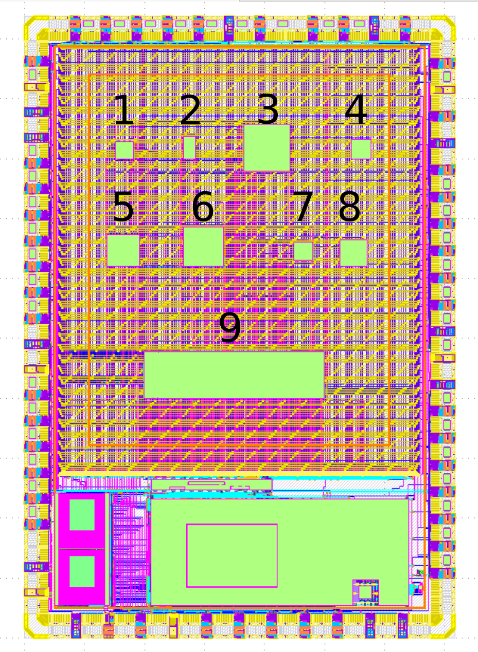
Finally in mid December all the designs were submitted and my first tape-out was complete!
Given the high level of interest in the tools and process I decided to make the Zero to ASIC course to teach other people what I had learnt. It was also a good opportunity to try a few new things I’d been thinking about; selling the product before having it, and flipped classroom style teaching.
I’ve always done a lot of work before trying to sell something, but there’s a risk that misjudging demand can waste a lot of time and energy. This time I put 15 tickets on sale in December for a course starting in February, and sold them in 2 hours! Demand was there!
Flipped classroom teaching is the idea that students watch pre-recorded lectures and then in the time they spend with the teacher go through areas that they need help understanding. I really like this idea because:
- The teacher can make great lectures with high production quality, and then not repeat themselves over and over.
- Students can study in their own time, which also works well for a course with global audience.
- The time together is spent focussed on exactly where the student is stuck, and leverages the expertise of the teacher.
In January I worked pretty much every day developing content and creating videos to support them. I had a chat with Joe FitzPatrick about how he structures his course content. In particular he records himself completing the labs and these ‘walkthrough’ videos become the 1st level of support, answering most questions before involving the teacher.
The course has been going really well, and we are just about to do a group tapeout with designs from the 1st 4 groups.
Feedback has been excellent:
I hope to continue running this course, learning more about chip design and meeting great people far into the future!